Tata Electronics signed a Memorandum of Understanding with ASML on May 16, 2026, locking in the world’s only producer of advanced lithography tools as the technology backbone for India’s first commercial 300-millimeter semiconductor fabrication plant. The signing was witnessed by Indian Prime Minister Narendra Modi and Dutch Prime Minister Rob Jetten during Modi’s state visit to the Netherlands, and pairs ASML’s equipment monopoly with the Tata Group’s ~$11 billion fab build in Dholera, Gujarat. The deal landed the same day as a broad semiconductor selloff on Wall Street that pulled ASML’s American depositary shares lower along with peers Nvidia and Intel.
What was actually signed
The MoU is a strategic framework, not a purchase order, but it commits both parties to a specific set of work streams: deployment of ASML’s lithography systems at the Dholera site, training programs for Tata’s lithography engineers, supply-chain coordination, and joint research infrastructure. Tata Electronics framed it as the agreement that “will ensure seamless operations at India’s first commercial 300mm semiconductor fab,” and ASML positioned the partnership as anchoring a long-running customer relationship across the entire equipment portfolio.
The transaction is the most concrete piece of news to emerge from Modi’s Netherlands trip, which has been organized around tightening commercial and technology ties with Dutch industrial champions. ASML, headquartered in Veldhoven, controls roughly 90% of the global lithography market and is the sole supplier of extreme-ultraviolet (EUV) machines used to print the world’s most advanced chips. For mature nodes — the segment where Dholera will operate — ASML’s deep-ultraviolet (DUV) systems dominate the installed base, and any greenfield 300mm fab globally is in practice an ASML customer by default.
Inside the Dholera fab
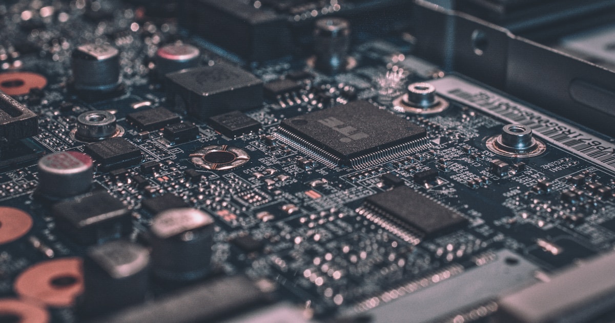
The fab is being built by Tata Electronics, a wholly owned Tata Group subsidiary, with original technology partner Powerchip Semiconductor Manufacturing Corporation (PSMC) of Taiwan. The project was approved by the Indian Cabinet in February 2024 under the country’s Semicon India Programme, which underwrites up to half of qualifying capital expenditure for approved semiconductor projects. According to the India semiconductor program summary, the Dholera build is sized at ₹91,000 crore (about $11 billion at current exchange rates) with planned capacity of 50,000 wafer starts per month at 28-nanometer geometries, with provisions to extend up to 90 nanometers for legacy products.
| Item | Detail |
|---|---|
| Location | Dholera Special Investment Region, Gujarat |
| Total project cost | ~₹91,000 crore (~$11B) |
| Wafer size | 300 mm (12-inch) front-end |
| Process nodes | 28 nm (primary); extends to 40–90 nm legacy |
| Capacity at full ramp | 50,000 wafer starts per month |
| Technology partner (original) | Powerchip (PSMC), Taiwan |
| Lithography partner (May 2026 MoU) | ASML (Netherlands) |
| Target end products | Power-management ICs, display drivers, MCUs, AI/automotive logic |
| First-chip target | Mid-2027 (subject to materials supply) |
A mature-node fab at this scale and geometry is not aimed at competing with Taiwan Semiconductor Manufacturing Company or Samsung Foundry at the bleeding edge. It targets the much larger by-volume market for chips that go into electric-vehicle inverters, industrial automation, smartphone displays, sensors, and the increasingly hot category of automotive-grade microcontrollers where supply has been the binding constraint since 2021. That product mix is precisely the gap India’s electronics manufacturers — including Apple’s contract assemblers operating in-country — have been pushing the government to fill.
Why ASML’s endorsement matters
Greenfield fabs are equipment-bottlenecked, not capital-bottlenecked. A single high-NA EUV system from ASML lists for north of $380 million; a fully tooled 50,000 WSPM 28-nanometer fab runs roughly $5–7 billion of equipment spend alone, the majority of which flows to ASML, Applied Materials, Lam Research, KLA and Tokyo Electron. ASML’s public order book and tool-allocation calendar are watched closely by the entire industry because there is no second source for its leading machines.
An ASML MoU on a specific fab project therefore matters at two levels. First, it signals that the project has actually crossed ASML’s internal commercial threshold — equipment allocations and engineer time get committed. Second, it raises the bar for Indian semi credibility globally: foreign customers and downstream integrators tend to treat “ASML-supplied” as a tacit reliability stamp on a brand-new fab from a country that has never run one.
The market backdrop ASML walked into
The same week the MoU was signed produced one of the sharpest semiconductor selloffs of 2026. ASML’s U.S.-listed ADR finished Friday, May 16 down 5.22%, on a day that saw the Nasdaq Composite drop 1.54% to 26,225, the S&P 500 fall 1.24% to 7,408.50 and the small-cap-heavy Russell 2000 shed 2.44%. The VIX rose 6.78% on broad de-risking. Single-name damage in chip world was worse: Nvidia closed off 4.42% and Intel off 6.18%.
Two narratives ran through the tape. The first was the “anticlimactic” Trump-Xi summit, which closed without the concrete trade or export-control concessions the market had positioned for. The second was a rates story: the 30-year Treasury yield ended the week above 5.1% as the long bond extended its sell-off, and high-multiple tech — ASML included — tends to trade inversely to long real yields. The MoU news, in other words, was bullish for ASML’s decade-long order book but had no chance of out-shouting the macro on a single Friday session.
Where the deal fits in India’s broader semi map
The Dholera fab is the headline asset but not the only one. India’s semiconductor mission has approved or backed at least five major projects over the last two years, with cumulative announced capex now well above $25 billion. The MoU with ASML mostly hardens the front-end fab leg of that strategy, while assembly/test (OSAT) and component manufacturing build out the rest.
- Tata Electronics – Dholera fab. 300mm, 28 nm primary node, ~$11B, ASML lithography, PSMC tech partner. First chip targeted mid-2027.
- Tata Semiconductor Assembly & Test (Assam). ₹27,000 crore (~$3.3B) OSAT facility in Morigaon, operational from 2025.
- Micron Technology (Sanand, Gujarat). $2.75B memory packaging and test plant; ground-broken September 2023.
- Tower Semiconductor – Adani (Panvel, Maharashtra). ₹83,947 crore (~$10B) analog/mixed-signal fab approved September 2024.
- HCLTech – Foxconn OSAT. Joint venture announced January 2024, smaller scale, targeting display drivers and chiplets.
What to watch from here
The MoU is a milestone, but milestones in fab construction are measured in years, not press releases. The signals worth tracking over the next twelve months are: (1) ASML’s quarterly bookings disclosure for any explicit India-allocation language in 2026 calls; (2) Tata Electronics’ capital-expenditure cadence in Tata Group consolidated filings, which will indicate whether equipment purchase orders are actually flowing; (3) the status of Indian critical-minerals and high-purity gas supply chains, which Tata management itself has flagged as the biggest schedule risk on the mid-2027 first-chip target; and (4) any updated Semicon India incentive disbursement announcements, which serve as a real-time barometer of Delhi’s political commitment to the program.
For ASML shareholders specifically, India is now another verifiable structural growth pocket alongside Arizona, Dresden and Kumamoto. It does not change the short-cycle picture — what moves the stock day to day is still EUV utilization at TSMC, the Chinese DUV restrictions debate and U.S. tech-tape positioning. But it adds one more multi-decade order book to a company whose investment case has always rested on the unmatched durability of its forward backlog.
Sources
- Semiconductor industry in India — India Semiconductor Mission projects and Dholera fab specs
- ASML Holding corporate profile — lithography market position, EUV monopoly
- Tata Electronics corporate profile
- India Semiconductor Mission (Government of India)
- ASML press-release archive
Disclosure: This article was produced with AI assistance and reviewed before publication. It is for informational purposes only and is not investment advice.